
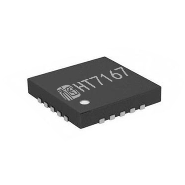
The HT7167 is a high-power density, fully integrated synchronous boost converter with a 16mΩ power switch and a 23mΩ rectifier switch to provide a high efficiency and small size solution in portable systems. The HT7167 has wide input voltage range from 2.7 V to 13 V to support applications with single cell and two cell Lithium batteries. The device has 12A switch current capability and can provide an output voltage up to 13V.
The HT7167 uses adaptive constant off-time peak current control topology to regulate the output voltage. In moderate to heavy load condition, it works in the PWM mode. In light load condition, the device has two operation modes selected by the MODE pin. One is PFM mode to improve the efficiency and another one is the forced PWM mode to avoid application problems caused by low switching frequency. The switching frequency in the PWM mode is adjustable ranging from 200kHz to 1.4MHz by an external resistor.
HT7167 could isolate the output from input side when shut down by a gate drive output disconnecting external FET, so that the load current consumption could be limited.
The HT7167 also implements a programmable soft-start function and an adjustable switching peak current limit function. In addition, the device provides 14V output overvoltage protection, cycle-by-cycle overcurrent protection, and thermal shutdown protection.
FEATURES
| APPLICATIONS
|
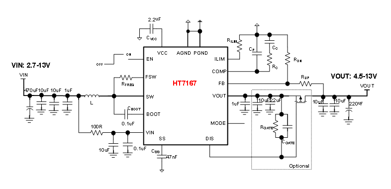
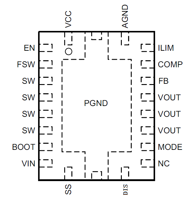
TERMINAL FUNCTION
Terminal No. | NAME | I/O* | Description |
1 | VCC | O | Output of the internal regulator. A ceramic capacitor of 2.2uF is required between this pin and ground. |
2 | EN | I | Enable logic input. Logic high level enables the device. Logic low level disables the device and turns it into shutdown mode. |
3 | FSW | I | The switching frequency is programmed by a resister between this pin and the SW pin. |
4/5/6/7 | SW | PWR | The switching node pin of the converter. |
8 | BOOT | O | Power supply for high-side MOSTFET gate driver. A ceramic capacitor of 0.1μF must be connected between this pin and the SW pin. |
9 | VIN | I | IC power supply input. |
10 | SS | O | Soft-start programming pin. An external capacitor connected to ground sets the ramp rate of the internal error amplifier’s reference voltage during soft-start |
11 | DIS | O | A gate drive output for the external disconnect FET. Connect the DISDRV pin to the gate of the external FET. Leave it floating if not using the load disconnect function. |
12 | NC | - | No connection inside the device. Connect these two pins to ground plane on the PCB for good thermal dissipation. |
13 | MODE | I | Operation mode selection pin for the device in light load condition. When this pin is connected to ground, the device works in PWM mode. When this pin is left floating, the device works in PFM mode. |
14/15/16 | VOUT | PWR | Boost converter output. |
17 | FB | I | Voltage feedback. |
18 | COMP | O | Output of the internal error amplifier, the loop compensation network should be connected between this pin and the AGND pin. |
19 | ILIM | I | Adjustable switch peak current limit. An external resister should be connected between this pin and the AGND pin. |
20 | AGND | - | Signal ground of the IC. |
0 | PGND | PWR | Power ground of the IC. |